A Simple Instruction Set Architecture
A considerable fraction of ISAs used to illustrate computer architecture texts are
based on the MIPS processors. This is a 32-bit processor (64 bits in its later incarnations)
with a register-to-register RISC architecture using 32 registers. The processor is
elegant and makes a popular vehicle for introducing the ISA and the pipelined architecture.
Here, we are going to create out own 32-bit processor and attempt to make is even
simpler ISA than MIPS. One simplification will be the structure of the proocessor.
We will reduce the apparent number of signal paths to make it easer to understand
the processor’s operation. Let’s begin with the ISA. Having decided to adopts a 32-bit
wordlength we have to balance instruction count, the number of registers, and the
length of literals.
It would be nice to have a 32-bit literal, 128 registers, and 512 instructions. This
would take an instruction 32 bits + 3 x 7 bits + 9 bits = 62 bits. That’s bigger
than 32 bits, so we don’t get what we want. What can we actually get?
Registers are the key. Too few registers and you are forever fetching data from slow
memory. Too many and you need an extravagant number of register select bits. Consider
the following:
Registers Address bits t Total bits Remaining bits
4 2 6 26
8 3 9 23
16 4 12 20
32 5 15 17
64 6 18 14
128 7 21 11
The three lines in read are the only viable options for a 32-bit op-code. Eight or
fewer registers would require excessive memory traffic. More than 32 registers would
either require a very short literal or a tiny number of op-codes. MIPS, SPARC and
the PowerPC have 32 registers, and ARM has 16 registers. Like ARM, we will choose
16 register, which leaves us with 20 bits for an op-code and a literal.
We will use a 12-bit literal. That gives us an unsigned range of 0 to 4,095. When
we do not require a second source register, we can combines those bits with the literal
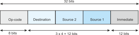
to give a 4 + 12 = 16-bit literal. The following figure illustrates the structure
of an op-code.
We are now going to create a microarchitecture. We will use a flow-through or single-cycle
structure; that is, a non-pipelined implementation. This matches typical MIPS-style
structures with five stages: program counter, instruction memory, register file (read),
ALU, data memory, register file (write). The register file appears twice because
the read operation takes part at the beginning of a cycle and the write operation
takes part at the end of a cycle.
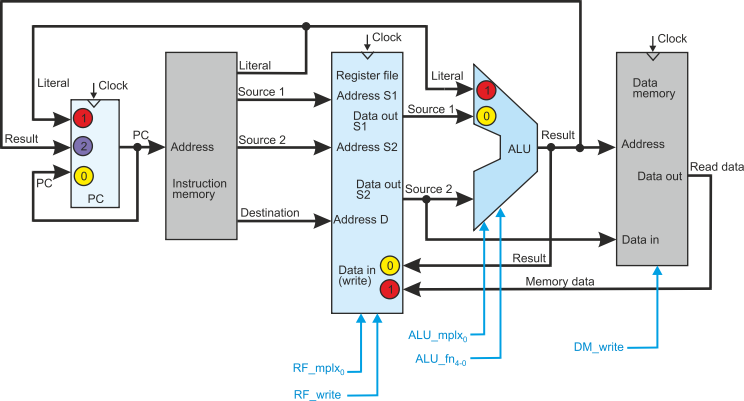
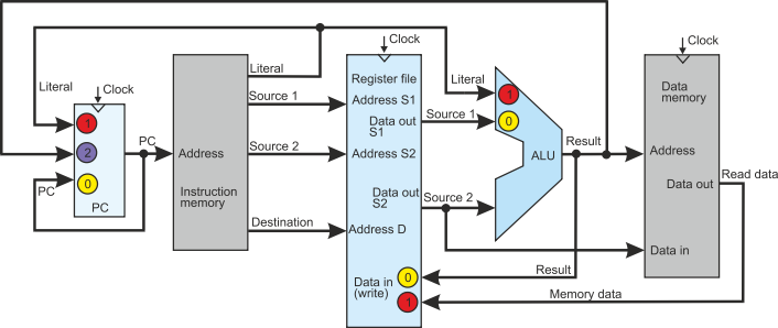
The following figure gives part of the structure of a processor. We have omitted
a few features for simplicity. In order to reduce the systems apparent complexity,
some circuits that normally appear explicitly have been incorporated in functional
units. There have been marked with colored circles. If you wish to see the sequence
of events taking place when a data-processing instruction like ADD r0,r1,r2 is executed,
click on the text in the blue box to the right.
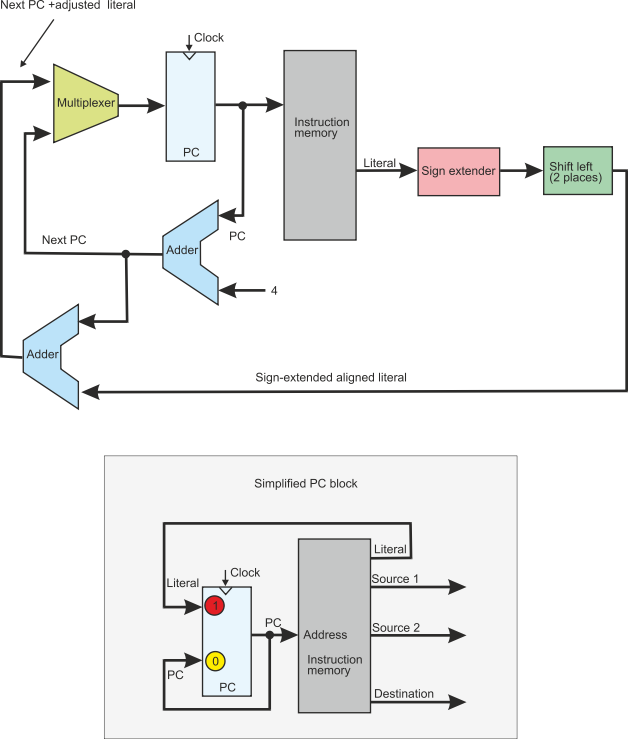
The figure below demonstrates how the conventional depiction of he PC path had been
simplified. The PC receives two inputs via a multiplexor. One is the sequential,
next instruction value that is the old PC incremented by 4 bytes to point to the
next instruction. The other is the branch value that consists of the incremented
PC plus the offset. However, the offset is not stored exactly because you can’t store
a 32-bit literal in a 32-bit op-code. First, the literal must be signed extended
to 32 bits; that is, the sign-bit is repeated to create a 32-bit value. Second,
because all branch addresses are aligned to a 32-bit word address, the two least
significant bits of the target are always zero. There is no point in storing these
two zeros in the literal field Consequently, the target address is stored as a word
value and then left shifter twice to create a byte value before adding to the PC.
The logic block below provides the circuitry which is normally included in the diagrams
of the organization of typical RISC ISAs. I have created a PC block (see below) that
includes all this logic in order to simplify the processor’s structure and to enable
the reader to better concentrate on the data flow.
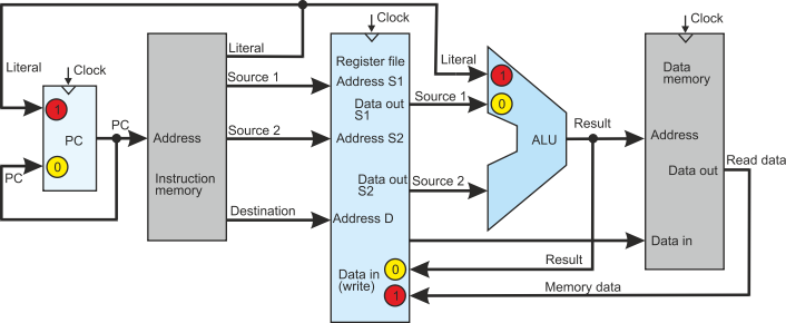
The next figure adds the ability to execute register-indirect jumps. A register-indirect
jump loads the program counter with the contents of a register (or even the contents
of a register plus an offset). This figure provides a new path to the PC block from
the output of the ALU (i.e., the result) to the PC. We now hve to include a three-way
multiplexor in the PC to include next sequential address, branch address, and jump
to register address.
We can now look at the control signals required to implements machine-level operations.
These are labeled on the following diagram.